This page was started on 08/17/03 and last updated 08/25/03
Hardware Quick Prototyping Modules
Note: This is all preliminary. These may/will change before I get the actual boards done.
Some background
For years I have had a need to quickly create electronic circuitry for experimentation. Like most other people I have gone through all the stages. Wire-wrap, soldering point-to-point, pluggable ProtoBoards. I have tried various methods for making my PC boards. Iron-on transfer, plotting directly on PC boards, tape on boards and various forms of photo etch. Even when I had good results I still had a single purpose board. Sometimes you can modify the board for another purpose, but there had to be a better way.
I had been contemplating creating modules with the old methods. Probably point-to-point wiring on perf board. But after seeing that people were having good luck with PC boards from places like www.apcircuits.com and www.olimex.com I decided to go directly to PC boards.
The place I wanted to start was with my video digitizer project. That project started by using an ImageWise Transmitter board (from the 1980s) and rewriting the firmware. Then I created my own design using TTL gates on a ProtoBoard. I put that design on a PC board. Next I created a version on a ProtoBoard using a Xilinx CPLD programmable logic chip. This worked as intended. But to add new features I needed to have more pins available on the CLPD. But I had used all of them. So to change it I would have to totally rewire it again.
I created a PC board layout for the CPLD version. But I never had it made.
The digitizer using a single CPLD.
All those connections
So I decided to create the modular design system around a larger CPLD device. And I needed a generic way to interconnect the modules. So how do you generically connect modules? What is the most efficient method? What is the fastest method? And it must be reusable. The point-to-point wiring on a ProtoBoard is fast and easy. (As long as you have a box full of prestripped wire.) But single wires get to be tedious. A good portion of the digital logic is based on busses. 4 bits and 8 bits is real common on small logic. So what if the interconnection is wider than one bit? What about 2 bits? 4 bits? 8 bits? 16 bits?
You can make the busses wider but you run into a case where you have too many wasted bits if you are making just a few connections. I finally settled on 8 bits per connector. This is optimum for 8 bit busses. If I need a 16 bit buss then I can use two 8 bit busses. But how do I keep from wasting wires if a module has two chips and each chip only has 1 or 2 connections that need connected to the CPLD? I can group these signals on to a single connector. Since the CPLD pins can be individually programmed for input or output I can match the random combining of signals. Another method is to have a connector that matches the 8-bit buss and the other end is separate (flying) leads. You can now route the individual wires any where you need them. And my final method is to have a box full of single wires. Each wire has a single female connector on each end. You can now connect any twoinividual pins in the system. (Assuming it doesn't already have an 8-bit connector plugged in the connector.)
Making the physical connection
So I arbitrarily chose a 10 pin header (2x5 pins) as my generic connector. This allows me to assign 8 data bits and I used the extra 2 pins as power and ground. The power and ground is available if I plug in a small module and I want it to be powered from the big module. So I artitrarily assigned the data bits starting at pin 1. So pin 1 is data bit 0. I then assigned +5v and ground to the last two pins. I later found out this is exactly the same pin-out as the Atmel STK300 eval board. What a stroke of luck!
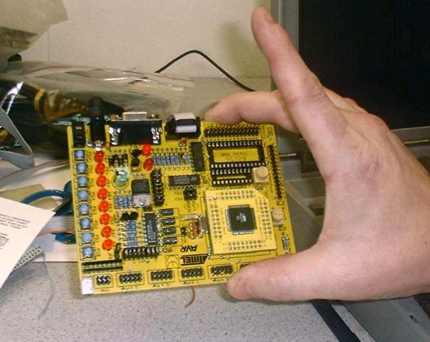
My STK300 board. It has the same 10-pin I/O connectors.
By using the 10-pin headers I can use 10-conductor ribbon cable for my interconnects. You can buy premade ribbon cables from DigiKey. I think they were $1.50 - $3.00 each. Another interesting point with the ribbon cables is that I can make a "multidrop" cable by crimping on more connectors. So, as described below, I can use a cable with three connectors to connect the output of the A/D to the data I/O of the RAM chip and also to an input connector on the STK300 processor board. So I have formed a buss with 3 devices.
[Pictures of various cabling methods]
So I think this method will work out real well. After I actually try it I may change my mind...
Using the digitizer project as a model, I wanted to create a CPLD board, a RAM board and a video input board.
[Perf board model]
[Block diagram of digitizer]
[Some description of digitizer]
[Pseudo code of processor code]
[Block diagram of next step]
[Block diagram of digitizer with subract and max intensity]
[Some other 'what if' block diagrams]
Click the images for a larger view.
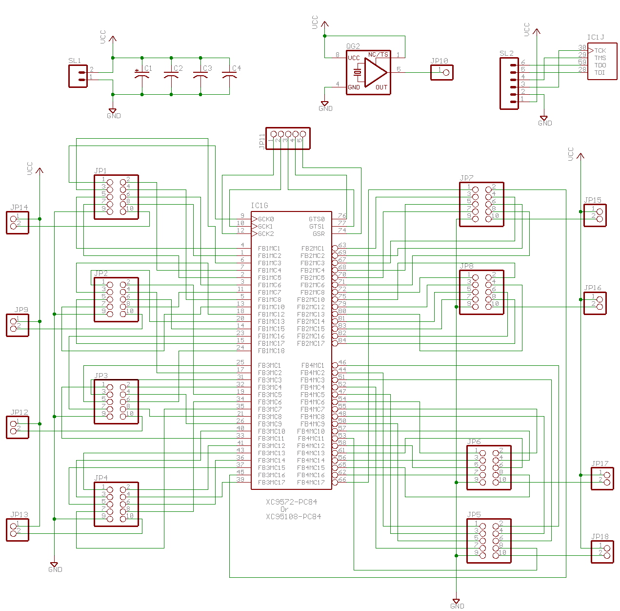
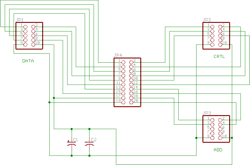
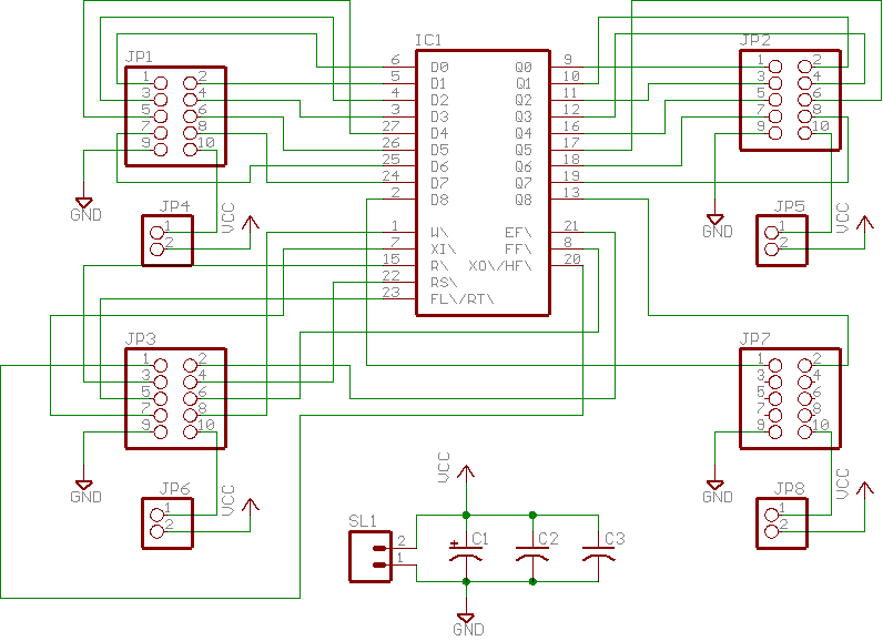
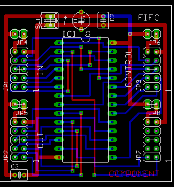
Eagle CPLD schematic
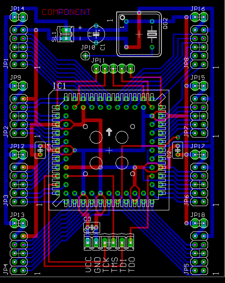
Eagle CPLD board
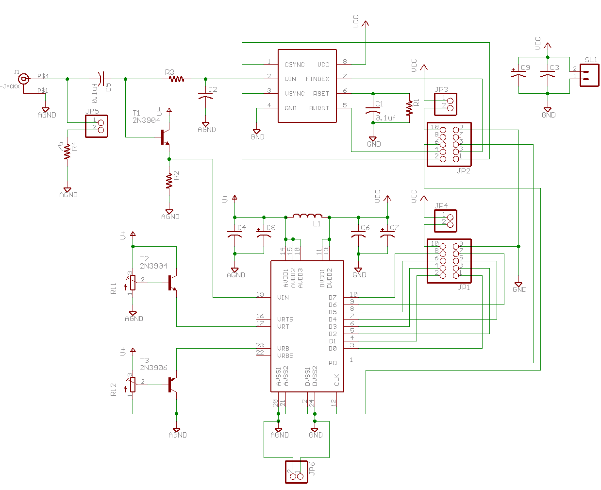
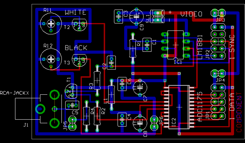
Eagle Video schematic
Eagle Video board
Eagle CMOS Video schematic
Eagle CMOS Video board
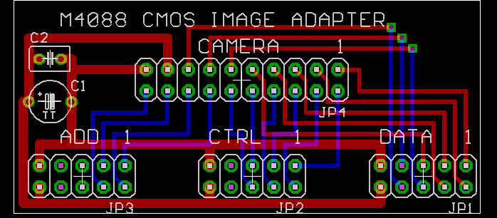
M4088 CMOS Image Board (PDF)
CMOS Image Chip (PDF)
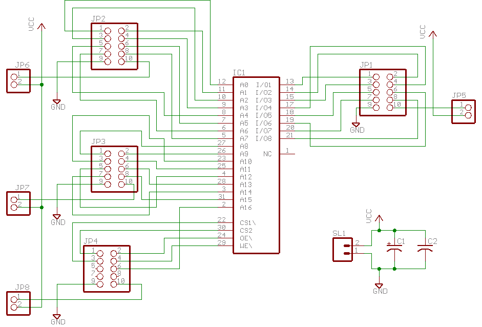
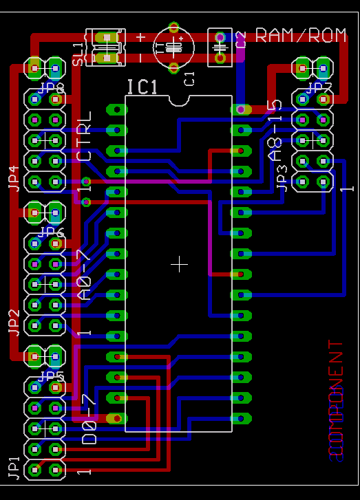
Eagle RAM schematic
Eagle RAM board
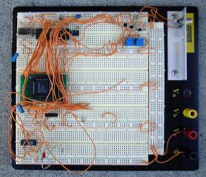
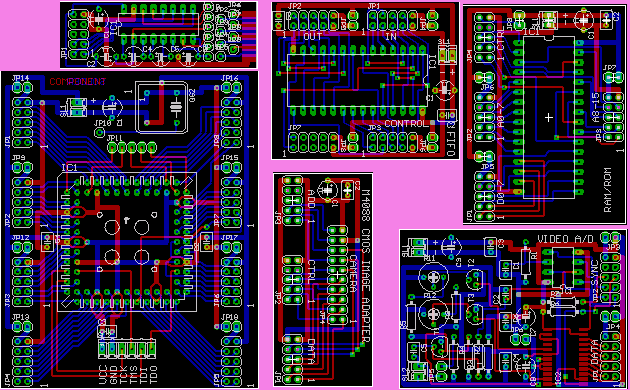
8/25/03 - After much playing around I almost have a my boards ready to send out. I tried to get the various boards to fit on a 6.3" by 3.9" panel to send to Olimex. They wouldn't fit. So I played with several boards to shrink them down. I had some extra room so I made an RS232 convertor board.
Below is the resulting panel. I still need to recheck everything and I will probably make a few more changes.
Visit Twin Cities Robotics Group
Back to my Home Page http://www.pobox.com/~jsampson
This page is currently maintained by Jeff Sampson